| bom | ||
| Gerbers | ||
| images | ||
| libs | ||
| sheets | ||
| .gitignore | ||
| fp-info-cache | ||
| fp-lib-table | ||
| ibom.config.ini | ||
| NeoGeoAES3_5-Layout.pdf | ||
| NeoGeoAES3_5-Schematics.pdf | ||
| NeoGeoAES3_5.kicad_pcb | ||
| NeoGeoAES3_5.kicad_prl | ||
| NeoGeoAES3_5.kicad_pro | ||
| NeoGeoAES3_5.kicad_sch | ||
| README.md | ||
| sym-lib-table | ||
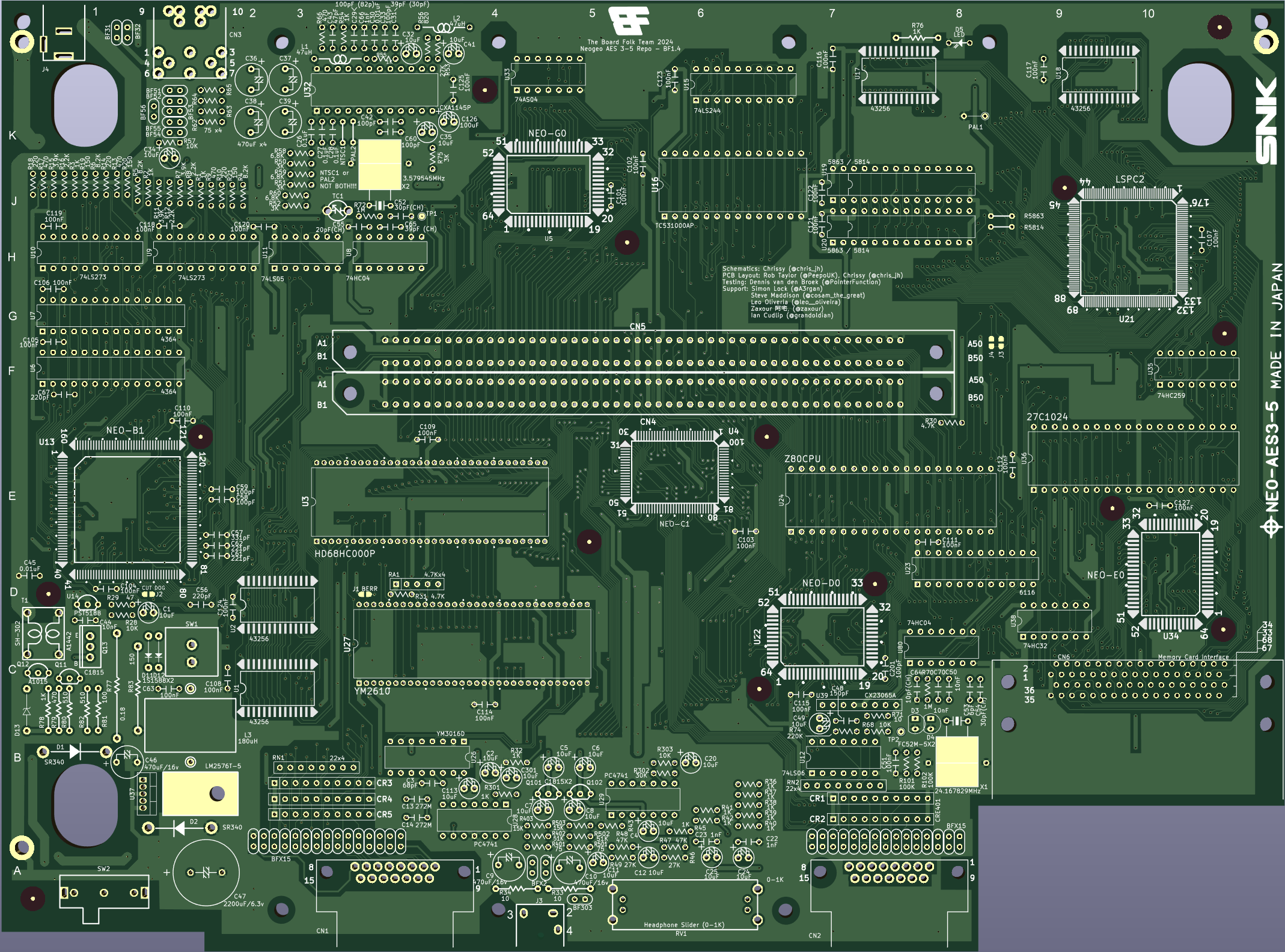
NeoGeoAES-3.5 PCB Reproduction
This repository contains a recreation of the main board PCB for NeoGeo AES consoles. This recreation is based on the available schematics for the NeoGeo AES and reverse engineering using scanned images of the original board's copper layers, so should be a reasonably accurate reproduction.
Revisions
| Revision | Tested | Comments |
|---|---|---|
| 1.1 | Working | Prototype |
| 1.2 | Not Tested | Added some missing silk screen |
| 1.3 | Tested | Moved some components on far right by 1mm to be in alignment |
| 1.4 | Tested (not by me) | Tweaks to BOM, updated Silkscreen |
Future Features
- Replace power section with something better
- Add RGB ByPass Mod
- Add Dual Controller component layput for using standard DB15
- Do a SMD Version
PCB Production
Minimum track widths, clearances and via sizes are within the standard offering of modern PCB fabricators. Development was done using JLCPCB and as such the Gerber files are provided to their specification.
The design is verified to work as a 2-layer PCB.
I have added it to the PCBWay Shared projects here

I recommend getting ENIG, but HASL will work also.
Bill of Materials
Most parts are marked on the board and it is expected that these will be reused from a donor board. It is completely possible that your particular board uses different (but compatible) parts so it's advisable to take photos before starting. For a complete BOM, consult the KiCad project's BOM folder, there you will find a CSV file or a PDF.
There are some components with mouser parts listed in Kicad BOM, DO NOT USE THESE. Need to verify they work.
9V or 5V
The NeoGeo AES 3-5 could come configured as either 9V or 5V supply input.
My board is 9V which this repository is based on. Due to this I have marked on the schematics/BOM which parts are not to populated if using 9V or 5V and by default the 5V circuit is N.F (Not Fitted).
C66 was also not populated.
Jumper / Links
There are various links around the board.
- NTSC1 / PAL2 - Only one of these should be populated, it would be very very very bad if both are populated
as one links to GND and the other to VCC.
- PAL1 and PAL2 - if your board is configured for PAL with the appropriate crystal, these should be populated
- NTSC1 - if your board is configured for NTSC, this should be populated with the appropriate crystal.
- 5863 / 5814 - depending on your memory type, one of these should be populated.
- J1 - BERR Signal into the CPU. Default is off.
- J2 - DOGE Signal into the NEO-B1. Default is off.
- J3 / J4 - This is for the EVEN signal to the LSPC2 chip. J3 is already enabled by default.
Memory
- 5814 - The shorter of the RAM Chips, make sure to populate into socket to the far right and populate the correct jumper.
- 5863 - The longer of the RAM Chips, uses the whole socket. Populate the correct jumper.
Thanks
- Rob Taylor (@PeepoUK) for doing most of
the PCB layout.
- Simon "Aergan" Lock (@Aergan),
Cosam (@cosam_the_great),
Dennis (@PointerFunction),
Leo Oliveria (@leo__oliveira),
Zaxour 阿宅, (@zaxour),
Ian Cudlip (@grandoldian)
for their insights, support and testing of the prototype boards.
- The rest of the Board Folk Team for their support and general
coolness.
- The NeoGeo Development Wiki for making
the original NeoGeo-2 Schematics available, and the people who maintain
this site.
Legal
As the product of this project is a replica of a proprietary product, the the author makes no claim of copyright to the schematics nor PCB layouts and releases these into the public domain, solely for the purposes of study and historical preservation.
You are free to produce PCBs based on this project's designs at your own risk and without limitation, for your own use or for sale and/or repair at a reasonable price. Attribution is appreciated. The authors are not obliged to provide support of any kind.
Under no circumstances will the authors be held responsible or liable in any way for losses, damages or costs resulting from the use of the information and/or resources of this project.
The resources are provided "as-is" without warranty of any kind, either expressed or implied, including, but not limited to, the implied warranties of merchantability and fitness for a particular purpose.